Sale!

XVME-100  RAM/ROM Memory Modulc

The XVME-100 RAM/ROM Memory Modulc is a singlc-high, VMEbus compatiblcboard,which can accommodate upto IMbyte Of RAM,EPROM,or maskprogrammablc ROM or 256K bytes of EEPROM, The modulc is designcd with an on.board battery backup circuit to provide power to CMOS RAM devices in the cventof a power failure.
The XVME-100 has eight 28/32-pin JEDEC sockets which are logically arranged as 2banks of 4 sockets cach, Each bank is designed to employ memory devices o’ thcsame type and speed,and each bank can be independently configured (.ia jumpers)in terms of:

Categories: ,

Description

Overview


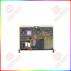
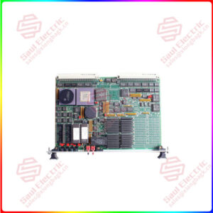
Essential details:XVME-100  RAM/ROM Memory Modulc

The XVME-100 RAM/ROM Memory Modulc is a singlc-high, VMEbus compatiblcboard,which can accommodate upto IMbyte Of RAM,EPROM,or maskprogrammablc ROM or 256K bytes of EEPROM, The modulc is designcd with an on.board battery backup circuit to provide power to CMOS RAM devices in the cventof a power failure.
The XVME-100 has eight 28/32-pin JEDEC sockets which are logically arranged as 2banks of 4 sockets cach, Each bank is designed to employ memory devices o’ thcsame type and speed,and each bank can be independently configured (.ia jumpers)in terms of:
VME Address/Memory Chip SizeAddress Modifier DecodeMcmory Deviee SpeedMemory Deviee PinoutMemory Backup Power
The XVME-100 RAM/ROM Memory Module has power down protection circuitrywhich prevents data from being written to memory when the voltage falls below4.75 Volts. The modulc also has the option of asserting SYSRESET under thiscondition.
1.2MANUAL STRUCTURE
The purpose ofthis first chapter is to introducc the user to the generalspccifications and functional capabilities of the XVME-100. Successive chapters wildevclop the various aspects of module installation and opcration in the followingprogression:

XVME-100

lf you need to inquire or purchase ,please send the product models to my email or call medirectly .

sunny  He

[Email] sales@xiongbagk.cn

[Mobile] 86-18059884797

[WhatsApp] 86-18059884797

[Skype] sales@saulcontrol.com

XVME-100  RAM/ROM Memory Modulc

2.1 INTRODUCTION
This chapter cxplains how to configure the memory module prior to installation in aVMEbus system, Included in this chapter is information on jumper options, jumperlocations,and power monitor circuit calibration and installation procedures.
2.2 LOCATION OF COMPONENTS RELEVANT TO INSTALLATION
The jumpers, memory sockets, and the Ebus Pl connector on the XVME-100Memory Module are illustrated in Figure 2-l. Figure 2-1lA show an cxpanded lcftside of the board, and Figurc 2-lB the right for clarification purposes.

The two banks are independently configurable, via jumpers to define five differentmemory module parameters,these parameters are:
、VME Address/Memory Chip SizeAddress Modifier DecodeMemory Device SpeedMemory Device PinoutMemory Backup Power
The following five subsections cxamines these jumper options in closer detail.
showing spccifically when and how jumpers should be configured.
2.4.1
VME Address/Memory Chip Size
12 jumpers cxist for cach bank (24 total)to definc the VMEbus address and mcmorychip sizc, Table 2-2 lists the jumpers and thcir definitions. The bank will occupya VMEbus address space of four times the memory chip size. The bank must bcassigncd to a boundarv which is a multiple of four times the memory chip sizc.