1 Year Warranty
Description
Overview
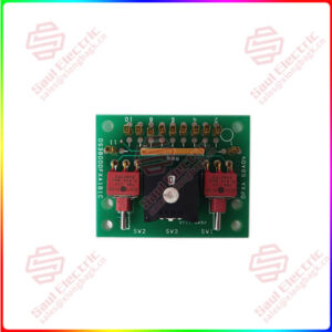
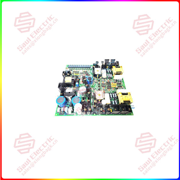
Essential details:DS200FGPAG1A GE Gate Pulse Amplifier Board
DS200FGPAG1A Technical Specifications
| Model Number | DS200FGPAG1A |
| Common Revisions | DS200FGPAG1AMD, DS200FGPAG1AKD, DS200FGPAG1AHD, DS200FGPAG1AFC |
| Series | LS2100 |
| OEM / Manufacturer | GE Energy |
| Part Specific Manual | GEI-100223 |
| Number of Test Points | 30, Nine for Gate A, Nine for Gate B, and 12 for Cell Status Monitors |
| Twelve-Pulse Convertor Supply Voltage | 2080 or 3300 VAC |
| Compatibility | Not Backwards Compatible |
| Number of Gate Driver Circuits | Two |
| Quantity of Fiber-Optic Connectors | 15, One Fiber-Optic Transmitter, and Fourteen Fiber-Optic Receivers |
Frequently Asked Questions about DS200FGPAG1A
What is the DS200FGPAG1A?
There are three main functions on the DS200FGPAG1A board. What are they and what do they do?
There are thirty test points on the DS200FGPAG1A board between Gate A, Gate B, and the test points for Cell Status Monitoring. What are the descriptions for the test points in Gate A?
What is the acceptable power input for the Gate Pulse Amplifier Board?
What sources supply gate currents to the push-pull circuit on the FGPA board?
lf you need to inquire or purchase ,please send the product models to my email or call medirectly .
sunny He
[Email] sales@xiongbagk.cn
[Mobile] 86-18059884797
[WhatsApp] 86-18059884797
[Skype] sales@saulcontrol.com
DS200FGPAG1A GE Gate Pulse Amplifier Board
Product Description
Gate Pulse Amplifier Board DS200FGPAG1A is from the LS2100 Series produced by General Electric Industrial Systems. This board has three primary yet basic functions to be used with the LCI (Load Commutated Inverter), these functions are SCR status monitoring, gate driver, and switching power supply. There are also three FGPA’s which are each for every three-phase silicon-controlled rectifier bridge. The power supply voltage on the DS200FGPAG1A should read at an input of 120 VRMs, and the approximate maximum voltage should read at 350 VA.
The SCR status monitoring of the DS200FGPAG1A is used to accumulate cell voltage information, this can be done with up to twelve FHVA devices. Once the voltages have been accumulated they will be sent through an optical data link back to the Load Commutated Inverter device. There are Status circuits within the FGPA model that are used to collect the voltage status that has come from the SCRs, since the polarity from the circuit is not specified the SCR could potentially be blocking the reverse or forward voltages.